
Understanding the Essentials of PCB Design
- Morgan Fletcher
- Sep 24, 2025
- 4 min read
Printed Circuit Board (PCB) design is a critical step in turning electronic product ideas into reality. Whether you are developing a simple gadget or a complex embedded system, understanding the essentials of PCB design process can save time, reduce costs, and improve product reliability. In this post, I will walk you through the key aspects of PCB design, share practical tips, and highlight how professional support can elevate your project.
What is the PCB Design Process?
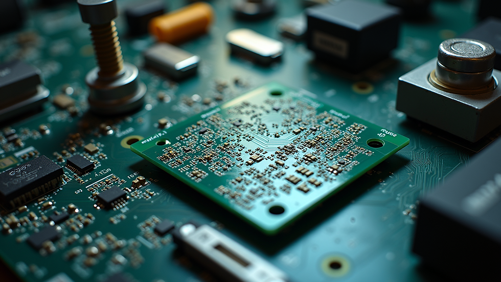
The PCB design process involves creating the layout and schematic that define how electronic components connect and interact on a physical board. It is more than just placing parts on a board; it requires careful planning to ensure signal integrity, power distribution, thermal management, and manufacturability.
The process typically includes:
Requirement Analysis - Understanding the product’s electrical and mechanical needs.
Schematic Capture - Drawing the circuit diagram that shows component connections.
Component Selection - Choosing parts that meet specifications and availability.
PCB Layout - Arranging components and routing electrical traces on the board.
Design Rule Check (DRC) - Verifying the design meets manufacturing constraints.
Prototype Fabrication - Producing a physical board for testing.
Testing and Validation - Ensuring the PCB functions as intended.
Final Production - Scaling up manufacturing for market release.
Each step requires attention to detail and collaboration between design engineers, manufacturers, and sometimes software developers.

Key Considerations in the PCB Design Process
When designing a PCB, several factors influence the success of your project. Here are some essentials to keep in mind:
Signal Integrity and Routing
High-speed signals need careful routing to avoid interference and signal loss. Use controlled impedance traces, minimize trace length, and separate analog and digital signals where possible. Differential pairs should be routed together with consistent spacing.
Power Distribution and Grounding
A solid ground plane reduces noise and improves signal quality. Use multiple power layers if needed and place decoupling capacitors close to power pins of ICs. Proper grounding techniques prevent ground loops and electromagnetic interference.
Thermal Management
Components that generate heat require adequate cooling. Use thermal vias, heat sinks, or copper pours to dissipate heat effectively. This ensures reliability and prevents premature failure.
Component Placement
Place components logically to minimize trace length and simplify routing. Group related parts together and consider mechanical constraints like mounting holes and connectors.
Design for Manufacturability (DFM)
Design your PCB with manufacturing capabilities in mind. Follow standard trace widths, spacing, and hole sizes. Avoid complex shapes or features that increase production costs or cause delays.
Testing and Debugging Access
Include test points and debugging headers to facilitate troubleshooting during prototype testing. This saves time and effort in identifying issues.
Tools and Software for PCB Design
Choosing the right tools can make the PCB design process smoother and more efficient. Popular PCB design software includes:
Altium Designer - Comprehensive and widely used in professional environments.
Eagle PCB - User-friendly and suitable for small to medium projects.
KiCad - Open-source and free, ideal for hobbyists and startups.
OrCAD - Powerful for complex designs and simulation.
These tools offer schematic capture, layout, simulation, and DRC features. Many also support 3D visualization to check mechanical fit.

How Professional Electronics Design Services Can Help
Navigating the PCB design process alone can be challenging, especially for complex or innovative products. This is where professional electronics design services come into play. They bring expertise in:
Optimising designs for performance and cost.
Ensuring compliance with industry standards.
Managing prototyping and small-batch production.
Integrating electronics with mechanical components seamlessly.
For example, BD Prototypes recently collaborated on a BLE-enabled smart zipper for YKK®, demonstrating how expert design and prototyping can bring cutting-edge ideas to market quickly and reliably.
Outsourcing to specialists also reduces risk and accelerates development timelines, allowing you to focus on your core innovation.
Best Practices for Successful PCB Design
To maximise your chances of success, follow these actionable recommendations:
Start with a clear specification - Define electrical, mechanical, and environmental requirements upfront.
Use modular design - Break complex circuits into manageable blocks.
Simulate critical circuits - Validate signal integrity and power distribution before layout.
Review and iterate - Conduct design reviews with peers or experts.
Prototype early - Test physical boards to catch issues before mass production.
Document thoroughly - Maintain clear schematics, BOMs, and assembly instructions.
By adhering to these practices, you reduce costly errors and improve product quality.
Moving Forward with Your PCB Design
Understanding the essentials of the PCB design process empowers you to take control of your electronic product development. Whether you are designing a simple sensor board or a complex embedded system, attention to detail and professional collaboration are key.
If you have an innovative idea, consider partnering with experienced electronics design services to bring your vision to life. From initial concept through prototyping and production, expert guidance ensures your product performs reliably and reaches the market faster.
Embrace the PCB design process as a vital step in your innovation journey. With the right knowledge and support, you can transform ideas into tangible, high-quality electronic products that stand out in today’s competitive landscape.


Comments